Despite the obvious hype, there is no doubt AI and semiconductors are key drivers of scientific and technological progress for the world for decades to come.
As silicon-based chips shrink toward their physical limits, the industry is desperately searching for alternatives to continue the progress defined by Moore’s Law — the trend that Intel co-founder Gordon Moore identified in 1965, predicting transistor counts would double roughly every two years with minimal cost increases.
New materials are being explored to replace the Silicon on which the semiconductors of today are built.
Photonic chip, using photon (particles of light) for data processing and transfer, is one option. Another option is to use the wide bandgap materials such as Gallium Nitride (GaN), Silicon Carbide (SiC), and Indium Selenide (InSe) to replace Silicon to process and transfer data faster and more efficiently – these are called third generation semiconductors.
Similar to Silicon, third generation semiconductors use electron for data processing but due to their physical properties, they are able to deliver higher performance with lower energy consumption. Many of the processing technologies used in silicon chip production can be used for the production of the third generation chips.
China has invested heavily in both photonic and third generation semiconductors, especially since the US tech embargo has affected its ability to build leading edge Silicon chips.
Its progress in Gallium Nitride (GaN) based semiconductor manufacturing has enabled Beijing to lead the world in military radar technology. https://huabinoliver.substack.com/p/chinas-rare-earth-ban-is-widening
Among third generation materials, Indium Selenide (InSe) has long been called the “golden semiconductor” as it offers an ideal combination of properties—low effective mass, high electron mobility, high thermal velocity, suitable bandgap for transistors, and a profile that can be ultrathin.
However, its wafer-scale integration has remained elusive due to the difficulty of precisely maintaining a 1:1 atomic ratio between indium and selenium during synthesis (called crystal growth). Traditional methods have only yielded microscopic flakes, insufficient for practical electronic applications.
In a landmark advancement, researchers from the International Center for Quantum Materials at Peking University in collaboration with Renmin University have achieved “a historic breakthrough in crystal growth”, according to reviewers at Science magazine where the research was published in July.
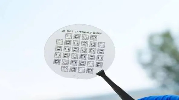
The team successfully fabricated wafer-scale two-dimensional (2D) indium selenide (InSe) semiconductors.
Led by Professor Liu Kaihui, the team developed a novel “solid–liquid–solid” growth strategy that overcomes long-standing barriers in 2D semiconductor manufacturing.
Published in Science under the title “Two-dimensional indium selenide wafers for integrated electronics,” the study demonstrates exceptional electronic performance, surpassing all previously reported 2D film-based devices.
The fabricated InSe transistors exhibit ultra-high electron mobility and a near-Boltzmann-limit subthreshold swing at room temperature, establishing a new benchmark for 2D semiconductors.
This breakthrough opens a new pathway for the development of next-generation, high-performance, low-power chips, which are expected to be applied widely in cutting-edge fields such as artificial intelligence, autonomous driving, and smart terminals in the future.
When the new InSe chip technology reaches maturity and enters into mass production, China will not only have won the chip war but have “exited the battlefield” altogether by mastering a new law of atomic physics.
Few will be surprised to learn that China dominates the global supply of indium and, by extension, controls much of the supply chain for indium selenide, as indium is its primary raw material.
Though indium is not a rare earth element, China has a dominant global share at over 60% which stems from its vast production and refining capacity, with the metal primarily extracted as a byproduct of zinc and lead smelting.
While this achievement won’t kill silicon tomorrow, it represents a genuine strategic leap. It signals that while the West has been focused on blockading the current technological paradigm, China is aggressively working to invent the next one.
The success of the Chinese research team reveals a profound story about the future of technology, geopolitics, and the very materials that will power our world.
Let’s unpack how the breakthrough is achieved, what it means for China, and the future of semiconductors.
Inside China’s InSe Wafer Breakthrough
InSe is a two-dimensional (2D) material, meaning it can form stable layers just a few atoms thick. For it to function as a high-performance semiconductor, it requires a perfect one-to-one atomic ratio of indium and selenium. Any deviation creates defects that ruin its electronic properties.
Unlike silicon, which is a robust, forgiving element that can be polished and doped into submission, InSe is unforgiving.
The achievement of the Chinese scientists was cracking this very problem. Their innovative method involves heating amorphous InSe film and solid indium in a sealed environment. The vaporized indium creates a liquid interface that allows high-quality, atomically perfect InSe crystals to form in a self-correcting process.
Crucially, they scaled this from microscopic lab flakes to 5-centimeter wafers and built functional transistor arrays, proving the material is “fabrication-grade.”
This is a vital step in moving a material from the lab to the factory, a bottleneck that has stalled many promising post-silicon candidates.
Promise of a ‘Golden’ Semiconductor
InSe, often referred to as a “golden” semiconductor, has long been a leading contender to replace Silicon as the material for future semiconductors as Silicon reaches its physical limits.
First, its electron mobility — the speed at which electrons move through it — is exceptionally high, far superior to silicon. The material’s high electron mobility translates directly to faster switching speeds and more powerful processors.
Research shows that transistors made with this material could triple the intrinsic switching speed of current 3nm silicon technology while improving energy efficiency by an order of magnitude.
Second, unlike the “wonder material” graphene, which has no natural bandgap and thus cannot be easily “switched off,” InSe is a true semiconductor with a tunable bandgap, making it suitable for digital logic.
Finally, its atomically thin nature allows for superior gate control, mitigating the “short-channel effects” that plague modern silicon transistors and cause power leakage.
Reality check – the silicon isn’t dead
Of course, it is far too early to pronounce the end of the current silicon-based semiconductor supply chain. Creating a perfect wafer is only the first, albeit critical, step. The magic of a modern chip lies in patterning trillions of transistors onto that wafer with nanometer precision.
This process depends on a mind-bogglingly complex and expensive ecosystem that China has yet to master domestically, including the EUV lithography machines.
Furthermore, the global semiconductor industry is a multi-trillion-dollar behemoth built on a silicon-based infrastructure that has been optimized over the past 50 years. The 5cm InSe wafer is a stunning proof-of-concept, but it is a world away from matching the 12-inch wafers that are the standard in modern fabs.
Transitioning the industry to new material will take years and hundreds of billions of dollars, with significant challenges in yield, cost, and reliability. Silicon will remain the workhorse of the digital world for the foreseeable future.
Not a knockout punch but a strategic leap to provide a superior alternative path
The true significance of this breakthrough is not that it renders silicon obsolete, but that it provides China with a powerful, sanction-proof path to developing next-generation technology for key strategic sectors where performance is paramount, and cost is secondary:
- Military and Aerospace: This is the most immediate and critical area of impact. For applications like advanced radar, electronic warfare systems, and satellite communications, InSe-based chips could offer a decisive performance advantage. By developing a sovereign capability in a “beyond-silicon” material, China can build specialized, high-end military, and superior hardware that isn’t dependent on western technology.
- AI, Cloud, and High-Performance Computing: The most significant commercial threat is to the dominance of companies like Nvidia. An InSe-native AI accelerator could offer superior compute performance per watt, a critical metric in the energy-hungry data centers that power the cloud and AI revolution. An InSe-native AI accelerator could enable Chinese firms to build powerful, efficient, and fully domestic AI supercomputers — a key national priority.
- Consumer Electronics and Medical Devices: In the longer term, InSe’s unique properties open up new product categories. Its superior flexibility makes it suitable for foldable displays and wearable electronics, and its sensitivity and low power consumption make it ideal for advanced medical sensors and Internet of Things (IoT) devices. InSe’s flexibility, sensitivity, and low power use create a market where China could leapfrog existing technologies and establish a new frontier of innovation.
- Impact on Existing Chip Companies: The incumbents aren’t obsolete, but they’re on notice. Firms such as Nvidia, TSMC and Intel must accelerate R&D in 2D materials to avoid being outflanked. Equipment makers like ASML will still find a market, as future InSe fabs will need lithography tools. But they need to work with Beijing, who controls the core chip design IP as well as the raw material supply chain. As mentioned earlier, China dominates global indium supply with more than 60% market share due to its massive zinc and lead smelting capacity.
The real losers are the sanctions, designed to trap China in the silicon paradigm, which it now has a credible path to sidestep.
China has not killed the silicon chip. However, the undeniable truth is this – a significant scientific breakthrough has occurred, and its geopolitical implications are profound.
China has not ended the chip war, but it has successfully opened a new front — one fought not with geopolitics and supply chains, but with fundamental materials science.
This achievement is a clear signal that a strategy based solely on containing an adversary’s access to existing technology is doomed to fail.
The future of computing will be determined not just by who can etch the smallest lines on silicon, but by who can master the atomic intricacies of the materials that will replace it.
By Hua Bin